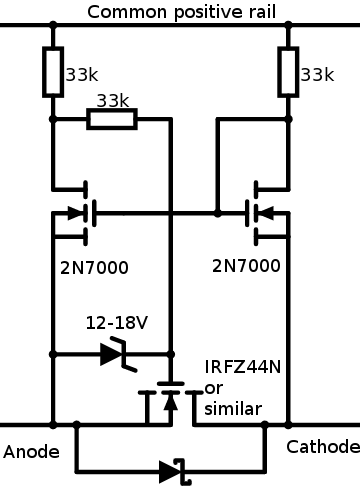
The schematic shown here is for an 'ideal diode.' This device uses active electronics to emulate a diode with a zero forward voltage drop. Ideal diode circuits are three-terminal circuits: Two connect in place of a standard diode, and the third supplies power for the circuit itsself. They most commonly find application as blocking diodes in photovoltaic systems or as part of a split-charge battery management solution in a boat or mobile home, and less often may be found serving as reverse-polarity protection. A well-known example can be found in the Raspberry Pi 3, which uses an ideal diode circuit very similar to this in order to prevent a powered USB hub from back-feeding power into a computer connected to the micro-USB power socket.
This circuit is unusual in being designed for low-side or common positive installation. This renders it of no use for boats or mobile homes - such installations are invariably common negative - but it does have a niche in photovoltaic power. For reasons relating to corrosion resistance in the event of a fault, many photovoltaic installations are set up using a common positive - multiple panels connected in parallel, positives together, but each with its own independant blocking diode on the low side to prevent current running in the wrong direction through a shaded panel.
Low-side installation also means it can use an N-channel MOSFET, which allows for even lower forward voltage drop than is possible with a high-side ideal diode of similar design, which in turn is already lower than a schottky diode can achieve.
This circuit is a form of high-gain differential amplifier. Such circuits are usually constructed using bipolar junction transistors rather than MOSFETs, but MOSFET's offer advantages in power consumption.
Some of the components are optional depending on usage. In low-current applications, the schottky diode may be omitted entirely - it serves only to protect the transistor from excessive heat dissipation in the body diode should the supply voltage be insufficiently high to pull the gate into saturation. In low-voltage applications, where it is assured that neither anode or cathode sides will go more than 20V below the common positive, the zener clamp diode and associated resistor may be omitted and the power MOSFET gate connected directly to the resistor-drain junction of the appropriate side of the circuit. Note that even '12V' solar panels can easily have an open circuit voltage in excess of 20V.
A more common design uses NPN bipolar transistors in place of the paired MOSFETs, but is otherwise identical. Note that the 2N2222 is not a suitable component for this application except at very low voltages (<6V), as the base-emitter junction has a very low reverse breakdown voltage - a difference in potential of more than seven volts between anode and cathode would lead to transistor failure in this manner. This variation, using 2N7000 MOSFETs, both avoids that failure mode and allows for the use of much higher value resistors with correspondingly low current consumption and so reduced energy use.
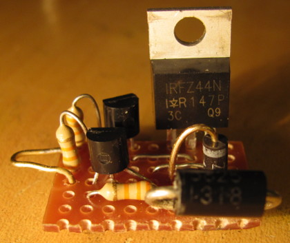
I have personally verified the circuit performs as intended both in simulation and in an actual prototype. Using an IRFZ44N power MOSFET, a forward drop of only 40mV at 2A could be achieved easily, with the circuit itsself drawing negligable power. Even so, any circuits constructed to this design should be tested before use, as it is very sensitive to component variation. If mass-produced, the only way to ensure consistent performance may be the use of a matched component package and 1%-tolerance resistors. Note the absolute value of the two paired resistors is not critcal, but the do have to match quite closely so that the circuit is 'balanced'.
So how does it work? Look at the right-hand side first, the 'cathode' side. This is a FET with a pull-up resistor, driving it's own gate. The higher the gate rises, the more the FET is turned on, which pulls the gate down. It's a simple negative feedback system which maintains the gate of the FET a constant voltage above the source terminal - on the order of 1.5V, depending upon the resistor value and subject to a significent amount of variation with temperature. This will always be a voltage within the linear region of the FET's operation, where it is neither fully on or off. That's the key. MOSFETs have a narrow linear region.
On the left-hand side, this voltage is applied to the other FET's gate, and this is where the magic happens: The Vgs of this FET varies with the anode terminal voltage. When the anode is at a greater potential than the cathode, Vgs is below that critical turn-on threshhold established by the right-hand side, allowing the associated pull-up resistor to bring the power MOSFET gate high and turn it on. But when the anode is below the cathode, the left-hand FET Vgs is increased above that theshhold, turning on the left-hand FET and so pulling the power MOSFET gate low, turning it off.
It's a very high-gain differential amplifier, but the gain is so high that for all practical purposes it is a comparitor. The final touch is a zener clamp - as very few power MOSFETs can take a Vgs above 20V, this just prevents damage under higher voltage conditions.
Design by Codebird, a variation upon a design already published in numerous locations, but most specifically upon that found on jiggerjuice.info