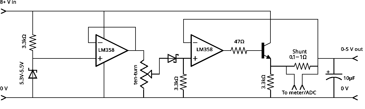
This document describes a design for a linear regulator variable power supply capable of maintaining very low output voltages - as low as just one milivolt, with a load regulation of 10mV/A. Maximum output voltage is 5V at 8V supply voltage. This power supply was designed for use in a specialised adjustable power supply intended primarily for testing of semiconductors, specifically measuring diode drop at varying current and MOSFET characteristics below the threshhold voltage in order to identify counterfeit components. For this purpose it includes an output shunt that, together with a common ADS1115 differential ADC, makes it easy to take continuous and highly precise measurements of output voltage and current - or the shunt can be simply connected to a panel meter.
This is not a high current supply. The circuit used for testing, when supplied with a stable eight-volt input, was able to maintain full output voltage up to a load of 350mA.
In most aspects this is a very standard linear voltage regulator circuit. The voltage reference is provided by a 5.3V to 5.5V zener diode, buffered by one half of an LM358 op-amp. This component is low-cost, readily available and able to operate correctly with input and output voltages very close to the negative supply. This is then supplied to a ten-turn precision potentiometer to set the output voltage.
The output of this potentiometer is dropped via a schottky diode. This feature is key to the low output voltage ability of the circuit. No potentiometer is perfect - between limited travel and wiring resistance, it is impossible to turn even a ten-turn pot to an output voltage of less than around fifteen milivolts. The forward drop of the schottky diode subtracts from this, allowing for a voltage of true zero to be selected. The reference zener needs to be corespondingly higher than the desired maximum output voltage. A consequence of this is that the effective current draw of the potentiometer becomes substantially higher when turned towards the higher end - thus the need for a voltage follower between the voltage reference and the potentiometer.
The regulator element itsself is a very common op-amp linear regulator using negative feedback, constructed from the second half of the LM358. This circuit is used very commonly, but may not be instantly recognisable as it is usually found inside of a component such as an LM317 or 78xx linear regulator. As none of these all-in-one regulators is capable of working at extreme low voltages, this same approach must be implimented with separate components for this supply.
The final part of the circuit is a power transistor. This is a simple power NPN bipolar with a 47Ω base resistor - while a MOSFET coud be used, it would require a far higher input voltage and so dissipate more power. Reducing the value of the base resistor may reduce the required input voltage slightly, but 47Ω has been confirmed experimentally as a workable value in conjunction with an MJE13005 transistor. Do not seek that specific part out as a recormendation - it was used only because it had recently been salvaged. A shunt is used for measuring output current, with feedback taken after the shunt so that any voltage drop across it will be compensated for by the regulator. A 1Ω or 0.1Ω shunt will be suitable.
This circuit has a minimum of components, all readily available. Capacitors on the input and output are optional, but will improve voltage stability if the load does not draw a steady current. The resistor values shown in the schematic have all been tested experimentally and found to work reliably, but it may be possible to use higher values and so slightly reduce current consumption of the regulator itsself.
Minimum supply voltage is limited by the LM358: Though it can drive its output right to the negative rail, it cannot drive it fully to the positive rail. Together with the need to bring the base of the power transistor at least a diode-drop above the output, this means that the input voltage must always be at least approximately three volts above the output voltage - exact value depending upon choice of transistor. This is still low enough that the circuit can be operated off of a 9V battery, but in practice the internal resistance of one such battery may be too high to maintain the required 8V at higher current draw and so two such batteries in parallel are needed.
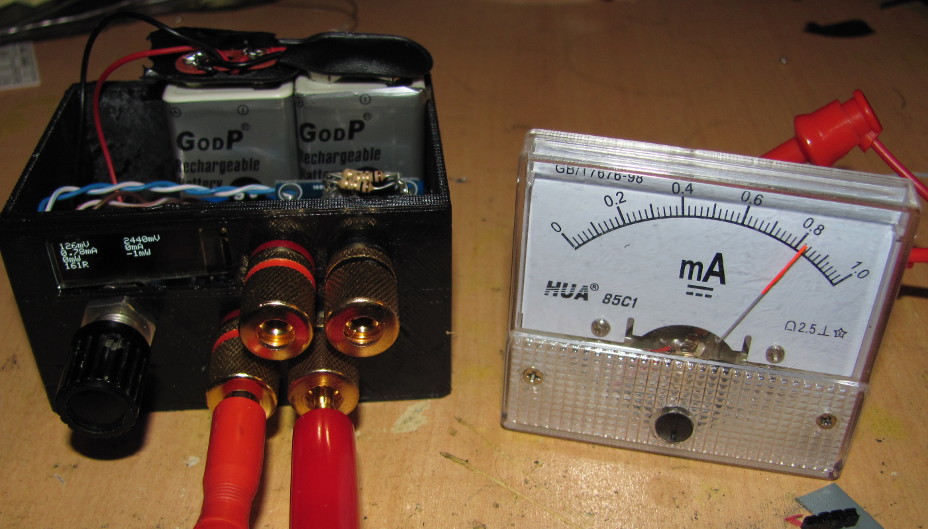
This circuit was used - in conjunction with an arduino pro mini, an ADS1115 differential four-input ADC and an OLED display for instrumentation - to construct this component tester. Demonstrated here testing the sensitivity of an analog one-miliamp meter. The remaining ADS1115 inputs are connected to additional banana sockets with a 1/4Ω shunt between them to serve as a low-voltage multimeter. The completed instrument can be used to measure and graph the forward drop of diodes while varying current, determine the threshhold voltage of MOSFETs, measure BJT gain and collector drop, measure resistance vs Vgs in the sub-threshhold region of MOSFETs and measure the DC offset and output range of op-amps. This makes it a useful general-purpose component tester.