All about ideal diode circuits.
Everyone knows what an ideal diode should be: It should have infinite resistance when reverse biased, and zero resistance with no voltage drop when forward biased. Such a diode, inconveniently, does not exist outside of textbooks. This is a shame, because there are many situations when one would be desirable.
As a solution to this there is the ideal diode circuit: The use of active electronics to emulate the properties of an ideal diode more closely than any real diode can.
There are several classes of ideal diode circuit, each with advantages and disadvantages. I shall describe the common ones here, including one of my own design. All of them rely on the same fundamental component: A power MOSFET. When the diode is reverse biased, the MOSFET is off. When the diode is forward biased, the MOSFET is turned on and the resistance falls sufficiently low that the voltage drop across the MOSFET becomes less than that of even the best Schottky power diodes. As well as these circuits there are some specialised components such as the LTC4358 which are dedicated to this function. This sounds like a simple enough task, but there are some practical considerations that make such a circuit a little difficult to design.
The main uses for ideal diode circuits are as replacements for Schottky power diodes in order to improve energy efficiency or reduce required operating voltage. They are often used as blocking diodes in solar power applications, or for split-charge configurations in boat or mobile home power systems to conserve some engine-starting power even if the main battery is discharged.
One critical word of warning for all these designs: Beware the MOSFET gate-source limit. Most MOSFETs die if you go over 20V. If you're using one of these circuits to prevent a 12V lead-acid battery from discharging, which is the most common application, that's not a problem. But if you're using higher voltages, you need to take this into account. The easiest way it to simply add a voltage regulator to the ground ('power') input - a 79L12 should be suitable.
An ideal diode does require a small amount of power to operate the active electronics, and for this reason the circuit has three terminals: Anode, cathode, and power. In most cases the power is intended to connect to a voltage some volts below the anode or cathode - this is simply to allow the circuit to be installed as a drop-in replacement for a schottky diode in a solar or split-charge application, where that diode would be installed on the positive wire between battery and solar panel or between two batteries. There is no reason an ideal diode operating off of a voltage above the anode/cathode could not be made, and the circuits below can usually be adapted with little difficulty if that is your requirement.
Direct comparator.
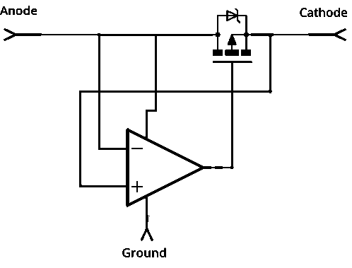
- Very low component count.
- Requires a expensive comparator of specialised properties.
This is the simplest, most obvious approach: Just compare the voltage each side of the MOSFET using an op-amp. It actually works, but it has a flaw: You will be comparing a voltage which is right at the supply rail with a voltage which will be potentially many volts above the rail, or only millivolts below. There are not many op-amps capable of doing this, and they are mostly expensive, and mostly only available in surface mount form - not hobbyist-friendly. Sure, it can work, but there are cheaper ways.
Divided input comparator.
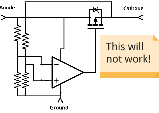
- Low component count
- Doesn't actually work.
The obvious solution to the above problem! But... sorry, this isn't going to work. You're looking at measuring a voltage difference of only a few millivolts: 1% resistors just aren't going to cut it. It's just not practical to achieve the required accuracy for a reasonable price using this method.
Transistor pair:
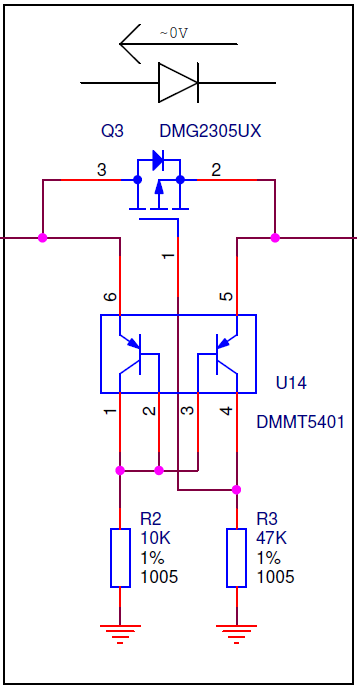
- Requires matched component pair.
- P channel only.
- Can take a bit of fine-tuning to prevent reverse leakage.
Unlike the above, this is actually practical.
A pair of bipolar transistors can operate as a comparator. The details of exactly how this works are rather complicated, but this configuration is at the heart of most comparator circuits. It works very well, but subject to a limitation: When measuring differences of millivolts, the transistors need to be identical. Absolutely identical. Beyond manufacturing tolerances. The only way to solve this is to buy a matched pair component: A pair of transistors encapsulated into one package, manufactured simultaneously, aged identically.
The example shown here is the input protection from the Raspberry Pi 2/3, using a DMMT5401 (Pi 2) or BCM857BS (Pi 3) matched pair. It's functioning is explained by Asmyldof on StackExchange. It's a very good circuit to prevent a Pi from feeding power back into a USB power supply and potentially damaging it. In this case a simple diode would not be possible, because the voltage drop would prevent the Pi operating off of a 5V USB supply, and so a ideal diode circuit is required.If the Left is low and the right is high R2 (and the left transistor a little) will negative-bias the base of the right transistor's base, allowing it to push the gate to the right voltage; closing the FET's channel and the body diode will block as well. If the right is low and the left is high, the left transistor's b-e junction will work as a diode and pull the base of the right transistor high enough to close off, allowing R3 to pull the gate low, opening the transistor. Initially the right side will start to be powered by the body diode, but quite quickly the channel's low on resistance will take over causing a very low drop.
It does work, but can take a lot of fine-tuning to get working reliably as it is quite sensitive. Even if it appears to work, it may still allow a small amount of current to flow through backwards. This is why you seldom see this design used as a solar blocking diode. It's also a P-channel only design.
Charge pump:
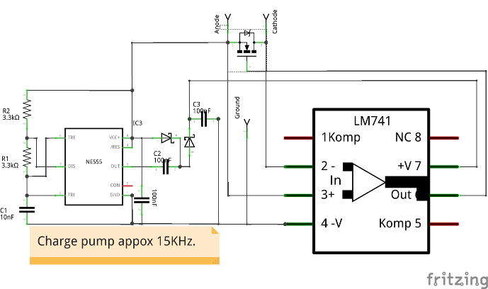
- Higher component count.
- Higher (5mA) current consumption.
- N-channel even in positive placement!
This is my own solution. This approach uses a comparator, but rather than require a comparator capable of operating with inputs at and above rail voltage it instead uses a charge pump to generate rails beyond the available input voltage. This adds complexity, but also removes all need for any unusual or specialised components: It's all common parts and everything is easily substitutable.
The charge pump requires an astable multivibrator, but any one will do. I used the classic 555 timer, but you could trivially redesign it to use a 40106 or any other astable multivibrator circuit. I used an LM741 for the comparator, but again this is easily substituted. The circuit is unusual for using an N-channel MOSFET for high side switching, something made possible by the use of the charge pump to supply above-the-input voltage. That means you can handle higher currents, with a very low on-resistance. Efficiency!
One down-side is the higher power consumption of the diode electronics - I measured 5mA on one I built, using a 555 timer IC and an LM741 as a comparator. I used 15KHz for the charge pump, but I believe it may work with a lower frequency to reduce power consumption. This power comes from the anode side though, so if you use it in solar power it isn't going to draw anything at night. You might be able to drop that a bit if you substituted a 7555.
There is one situation in which this solution is just about perfect: If you have a suitable driver available 'for free' elsewhere, as might be the case in, for example, a solar charge controller where a spare PWM pin on the microcontroller is trivially configured to provide the required square wave for the charge pump. In this case your high-reliability ideal diode requires nothing more than a low-cost op-amp chip, two capacitors, two diodes and a MOSFET.
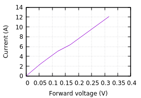
My breadboard testing achieved a forward drop of 0.31V at 12A, which is comparable to the best Schottky diodes at that current - but this was on breadboard with considerable resistance, and using an IRFZ44N MOSFET. Lower Ron parts are available. With a better MOSFET and on PCB, a lower drop should be easily achievable. I believe almost all of my measured drop was from the breadboard contacts.
I have produced a Fritzing schematic (Plus LM741 part) and PCB layout files. I've never actually made a PCB before, but I think these will work. Don't forget the negative voltage regulator if your supply voltage might go over 20V!